: Dr. Maria Baskin, Lishai Shoham and Prof. Lior Kornblum")
The development of high-performance alternatives to silicon in microelectronics has been brought nearer by researchers at the Technion-Israel Institute of Technology in Haifa who stretched an oxide material at an atomic level, thus controlling its conductivity. They said this is a “milestone advancement towards making efficient switches, which are the basic building blocks of computer chips.”
Researchers in the Viterbi Faculty of Electrical and Computer Engineering have been able to control an emerging material that they regard as a possible future alternative to silicon in microelectronics. This is a timely development, because scientists and engineers face challenges in continuing the transistor shrinking trend – an important driver of computer chip performance. They published their findings in the journal Advanced Functional Materials under the title “Bandwidth Control and Symmetry Breaking in a Mott-Hubbard Correlated Metal.”
Integrated circuits, more commonly known as computer chips (or simply chips) are at the core of modern life, responsible for processing, storing and transferring massive amounts of data. Chips are involved in countless tasks including vaccine development, spacecraft designs, Internet infrastructure, big data, autonomous vehicles, artificial intelligence, and the Internet of Things.
The continuous performance improvement of these chips has been driven by shrinking the size of the most basic logic “Lego” piece – the transistor, which is a miniature switch that controls the flow of electric currents; this is analogous to a faucet controlling the flow of water.
Already in the early 1960s, Intel founder Gordon Moore suggested that the transistors’ miniaturization rate should allow doubling of the number of transistors per area every two years. This prediction, named “Moore’s Law,” has dictated the miniaturization rate for decades. Modern chips now contain billions of transistors on about a square centimeter. In 2007, Moore declared that his law would come to an end within a few years. The CEO of Nvidia expressed an even more pessimistic view last year, saying that “Moore’s Law is dead,” a view shared by other technology experts.
Prof. Lior Kornblum of the Viterbi Faculty explained that, “as a result of the continuous miniaturization, modern transistors are only a few dozen atoms across. Because they are already so small, continuing miniaturizing without compromising their performance is becoming increasingly challenging. On the nanometric scale, the transistors behave in new ways that are different than their larger predecessors.”
One example of this problem is leakage of electric current when the transistor (switch) is supposed to be off. Kornblum noted that “it can be compared to a leaking faucet, multiplied by a billion; this could result in a lot of wasted ‘water.’ In a modern phone with billions of transistors, the tiniest current leakage will accumulate into a considerable waste of energy. This could quickly drain the battery and cause excessive heating of the device. Zooming out, when thinking server farms and data centers, the energy waste can be substantial and produce considerable heat.”
There are multiple approaches and strategies to tackle these challenges. One promising direction is the search for alternatives to silicon, the workhorse of today’s chips. Kornblum’s research group is studying various oxide materials, one of which can switch from being an electrical conductor to an insulator and back. The researchers want to harness this property for future transistors that could potentially switch more efficiently.
New tech demands precise control of material properties
Developing such a technology demands precise control of the material properties. The Technion team showed a route for manipulating the material’s electric properties by precisely controlling the distance between its atoms. Lab manager Dr. Maria Baskin achieved this by using a unique oxide growth system, depositing layers of atoms one on top of the other to grow films of the material. Thanks to this delicate growth process, she was able to set the distances between atoms with a picometer (one-thousandth of a nanometer) precision. In comparison, the distance between two atoms in silicon is approximately one-quarter of a nanometer (250 picometers).
“Every morning, I come to the lab and ‘fire-up’ the system,” said Baskin. “We can choose from a variety of atoms, control their arrangement and the spacing between them. Using these capabilities, we can even create materials that did not exist before, with a broad range of properties per our requirements.”
“The tools we’ve developed for the oxides growth are unique,” added Kornblum, who heads the lab. “Oxide growth is only the first step. From there, the graduate students start their research. Some focus on the materials’ physical properties, striving to understand how they function, and some utilize these materials to fabricate electronic devices that we hope will revolutionize microelectronics, renewable energy and other fields.”
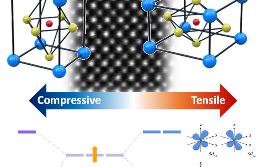
Doctoral student Lishai Shoham’s research deals with both of these aspects. She is studying the material’s properties and fabricating transistors from it, aiming to evaluate how it can be harnessed for microelectronics. In her latest scientific publication, Shoham led a team of a dozen other researchers from eight research institutions and companies in Switzerland, Japan, France, and the US. The team showed that by stretching the material at the atomic level, the elongation of the chemical bonds between the atoms changes the electrical properties: stretching by less than 2% of the atomic bond length, the researchers reduced the electrons’ tendency to hop from atom to atom. This stretching changed how the atoms were arranged in space. Through these tiny changes, which take place at a scale of one picometer, the researchers developed the groundwork for controlling the material’s transition from a conducting state to an insulating state.
Shoham concluded that “it’s is amazing to see that such minute changes in the material’s atomic structure have such a big impact on the electrical properties. We took this material to a synchrotron in Switzerland and saw how these tiny alterations affect the electrons’ arrangement in the material, as well as their behavior. These are the scientific foundations we need to develop future transistors from these unconventional materials. Today, I am implementing the results of our research on related materials, from which I am developing a new type of transistor.”